
New E-Beam Writer Enables Next-Generation Biomedical and Information Technologies
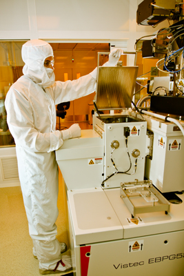
San Diego, Aug. 12, 2013 -- The new electron beam writer housed in the Nano3 cleanroom facility at the Qualcomm Institute is important for electrical engineering professor Shadi Dayeh’s two major areas of research. He is developing next-generation, nanoscale transistors for integrated electronics; and he is developing neural probes that have the capacity to extract electrical signals from individual brain cells and transmit the information to a prosthetic device or computer. Achieving this level of signal extraction or manipulation requires tiny sensors spaced very closely together for the highest resolution and signal acquisition. Enter the new electron beam writer.
|
Bioengineering professor Todd Coleman will use the new e-beam writer as one essential step in the building of his epidermal, or tattoo, electronic devices. The devices are designed to acquire brain signals for a variety of medical applications, from monitoring infants for seizures in neonatal intensive care to studying the cognitive impairment associated with Alzheimer’s disease or dementia, and soldiers struggling with post-traumatic stress syndrome.
Electrical engineering Ph.D. candidate Andrew Grieco is using the machine to develop a new type of optical waveguide that promises to improve efficiency and reduce power consumption. Grieco works in the laboratory of Shaya Fainman, professor and chair, Department of Electrical and Computer Engineering. Developing on-chip optical networking devices such as waveguides, switches and amplifiers is a critical step in the development of optical chips. Although information systems rely primarily on fiber-optic networks to connect and share data around the world, the underlying computer technology is still based on ele ctronic chips, causing data traffic jams.
|
Dayeh said technologies enabled by the e-beam writer will be important in local efforts to conduct research under President Obama’s BRAIN Initiative, which will require developing much smaller sensing and stimulating elements with higher resolution on chips the size of a few millimeters. “Current state-of-the-art electro-neural interfacing technology enables sensing from hundreds or thousands of neurons. If you want to understand the neurophysiology on the individual cell basis then we need to develop sensors that have the spacing of a few tens of nanometers, which is about one-hundredth the size of a neuron and is on the same scale as their synaptic connections,” he said.
Electron beam facility is open for business
UC San Diego’s new Vistec Lithography EBPG5200 electron beam writer is available for use by campus researchers, as well as industry and research partners. The e-beam writer, used for nano and micro-fabrication is a new addition to the Qualcomm Institute’s Nano3 facility, which provides a synergistic environment for fundamental research and development efforts at the nanoscale with a focus on nanoscience, nanoengineering and nanomedicine. In addition to providing essential nanofabrication capabilities for research on electronic and photonic materials and devices, Nano3 facilitates the pursuit of research in emerging, interdisciplinary and rapidly growing fields such as biomedical and biochemical devices, monolithic and heterogeneous integrated electronic and photonic devices and circuits, and sensor technology.
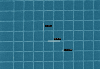
The new e-beam writer enables researchers to write fine features on a scale of less than 8 nanometers, over a large surface area up to 8 inches. The challenge of writing over large fields with electron beams is that the beam of electrons can become larger and diffused, distorting the features of the pattern. However, the EBPG5200 has superior electromagnetic focusing capability for extremely narrow electron beams over 1x1 mm2 write fields and a high stitching accuracy, which allows ultrascaled features to be written not only on research scale samples but also on commercial and production size wafers.
Adding the Vistec e-beam writer to Nano3 was enabled by funding from the Major Research Instrumentation program of the National Science Foundation, with contributions from UC San Diego, the Jacobs School of Engineering, the Department of Electrical and Computer Engineering, the UC San Diego School of Medicine, and Nano3 at the Qualcomm Institute.
Related Links
Nano3
Qualcomm Institute of Calit2
Shadi Dayeh Lab Page
Electrical and Computer Engineering Department
Bioengineering Department
Media Contacts
Catherine Hockmuth, Jacobs School of Engineering, 858-822-1359, chockmuth@ucsd.edu