Are Racks-on-Chip the Future of Data Centers?
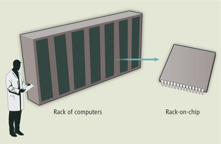
San Diego, Nov. 3, 2013 -- Increasing the scale and decreasing the cost and power of data centers requires greatly boosting the density of computing, storage and networking within those centers. That is the hard truth spelled out in the journal Science by faculty from the Jacobs School of Engineering at the University of California, San Diego.
|
In order to shrink data centers down to the size of a chip, a new data center network design is needed. “These integrated racks-on-chip will be networked, internally and externally, with both optical circuit switching (to support large flows of data) and electronic packet switching (to support high-priority data flows),” according to the article, “Directing Data Center Traffic.”
|
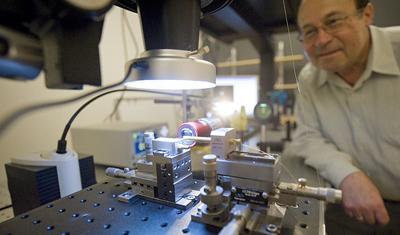
Industry is looking for ways to integrate optical networks densely within multicore processors, but Porter and Fainman – both of whom are affiliated with Calit2’s Qualcomm Institute at UC San Diego – argue that there are other challenges to overcome before that will be possible.
“Next-generation data center designs built with rack-on-chip designs will need to support both circuit and packet switching,” according to the Science article. Its co-authors make the argument that each processor in the rack-on-chip design must have a transceiver, which converts the electrical signals in the processing core with the optical photons that travel through fiber-optic cables – which would require shrinking them small enough to integrate with the rack-on-chip.
To prevent overheating, the transceivers need to be “low-power and highly efficient,” so that only a small number of photons traveling a short distance should be needed to represent a bit of information.
Nevertheless, for all the recent advances in nanophotonics and silicon photonics, “the efficient generation of light on a silicon chip is still in its infancy,” noted the researchers, adding that they “may not be able to overcome the fundamental issues prohibiting efficient generation of light in indirect band-gap semiconductors.”
|
According to Fainman and Porter, the technology could eventually deliver online applications to hundreds of millions of users, and enable big-data applications such as computational climate modeling.
How far in the future? Asked after the Science article’s publication, CNS’s Porter was realistic: “We’re excited about the potential of using cutting-edge photonic devices in data center networks, but the process of determining just what capabilities those devices should have, and then working with physics and engineers to actually build and integrate them, is a decade-long undertaking.”
Related Links
Science Article
Jacobs School of Engineering
Electrical and Computer Engineering
Computer Science and Engineering
Center for Networked Systems
Qualcomm Institute at Calit2
Media Contacts
Doug Ramsey, 858-822-5825, dramsey@ucsd.edu


