
UCI Division Director Yee Discusses Nanoimprinting at UCSD
|
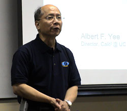
3.03.04 -- At the invitation of the Electrical and Computer Engineering department, UCI Division Director Albert Yee presented a seminar at UCSD on nanoimprinting last Friday. This event was held in tandem with the Jacobs School of Engineering's annual Research Review.
Nanoimprinting is defined as using an imprinting technique to create nanostructures. With photolithography successfully producing sub-100-nm structures, attention has now turned to 50-nm structures.
In his talk, Yee reviewed nanoimprinting techniques using polymers and described recent advances in the development of techniques for fabricating 3-D structures produced by a collaboration between the Institute of Materials Research and Engineering (IMRE) in-Singapore, which he directed for the last few years, and the University of Michigan.
Conventional nanoimprinting lithography is an embossing technique that combines the benefits of mass-production capabilities, cost efficiency in production costs, and the ability to produce structures well beyond the diffraction limit. The motivation for creating this kind of lithography technique is due to the cost of optical lithography systems -- well over $1B -- not to mention the inability to go down to 50 nm using such systems.
The advantages of nanoimprinting lithography are many. First, it has no diffraction limit: Features as small as 10 nanometers have been fabricated. Second, a broad range of materials can be used, including polymers, metals, and ceramics, which constitute key elements of many devices. Third, nearly any researcher working in this domain can perform this technique without needing a specialized fabrication facility or clean room.
But the challenges are daunting. It's extremely difficult to build a 3-D structure because of the many steps needed for material deposition and removal. It suffers from throughout and defect density problems. The technique has been demonstrated as yet for only a limited number of commercially available polymers. Very high temperatures/pressures are needed to cause the viscosity to drop for the polymer to flow into channels, but, as the temperature increases, the polymers, as well as the structures they form, degrade.
|
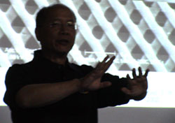
To eliminate the viscosity problem, the IMRE/U Michigan team devised a technique known as reversal nanoimprinting, in which the polymer is spin coated on the mold, then the polymer is transferred to the substrate. "The idea is that, by controlling the process," says Yee, "you can control the resulting structure."
Yee described the contributions of the Chemistry community (to complement those of the Electrical Engineering world) as using a "series of tricks" in surface treatment to enable more exact inking of a pattern on a surface. The advantages of this technique include that it can be done at lower temperature/pressure, inking can create a pattern that doesn't require etching, the technique can be used to print on a patterned or curved surface or flexible material, and the inking can be done in layers, which avoids the solvent mixing problem.
It's possible now to make 2-D structures, but what about 3-D? Others have created one-off 3-D structures using techniques that are slow, serial, difficult - and ultimately not practical. The technique described here, however, can be used to build 3-D structures of larger scales and at a higher throughput.
The inking technique is based on detailed numerical analysis and optimization of the geometry to cut the pattern. "In fact, we use a 'cookie cutter' approach," says Yee, "It's just that our cookie cutters are nanometer-sized. We've used finite-element analysis to calculate the stresses and geometries that would result in the smooth and precise cutting of these patterns." It's also possible to lay patterns over a substrate with a complicated topography, "like a KitKat candy bar," says Yee with a smile.
This technique eliminates the need for multiple layers, requires fewer processing steps (which should reduce fabrication costs), and makes it possible to create structures with sealed cavities (not currently possible using conventional nanoimprinting or semiconductor fabrication techniques).
In a biomedical applications project, Yee has used this technique to produce a substrate texture and evaluate the effect of the texture on cell growth and adhesion, specifically with muscle cells, which he describes as "very big and easy to visualize." His results also indicate, though, that the technique has the same effect on neuronal cells.
"We know cells can be guided by micro patterns," says Yee, a materials scientist by training and research background. "What we don't know is whether this works with nano patterns." According to biologists he works with, cells must understand patterns because they interact with the surface on which they're placed. "Cells secrete molecules that send out scouts to look at the surface to guide the cell on what to do next," says Yee. Some patterns can be confusing and, as a result, the cells do nothing. At other times, they line up in a certain direction, then migrate in that direction. "So there must be ways of controlling such growth," says Yee.
Yee summarized his talk by saying it's possible to fabricate nanostructures using a basic understanding of physics and materials under conditions that don't destroy the functionality of the polymers. But one needs a working knowledge of surface chemistry. This work has potential application to microelectronics, high-definition displays, photonics, micro- and nanofluidics, tissue engineering, and bioMEMS.