

Calit2?s Nano3 Lab Brings Cutting-Edge Cleanroom Facilities to Academic, Industry Users in San Diego
By Tiffany Fox, (858) 246-0353, tfox@ucsd.edu
San Diego, Calif., Nov. 5, 2008 — Sometimes it pays to think small.
Researchers at UC San Diego's Nano3 Lab are out to prove that nanostructures — objects one million times smaller than the diameter of a human hair — can have a giant impact on science, technology, medicine and the economy.
|
Despite its popularity among both UCSD scientists and industry researchers, the university's Nanofabrication Cleanroom Facility (better known as Nano3) remains a well-kept secret within the San Diego community. The lab, which is based in the UCSD division of the California Institute for Telecommunications and Information Technology (Calit2), has been in operation since May 2006 and currently serves more than 60 research groups from seven academic departments on the UC San Diego campus, including the Departments of Electrical and Computer Engineering (ECE), Mechanical and Aerospace Engineering (MAE), Bioengineering, Physics, Chemistry and Biochemistry, as well as the Jacobs School of Engineering's new Department of NanoEngineering, the Scripps Institution of Oceanography and the UCSD School of Medicine.
Nano3 derives its name from three emerging research areas: nanoengineering, nanoscience, and nanomedicine. "Our name suggests that we intend to bring scientists, engineers and medical doctors together to promote interdisciplinary research," remarks Yuhwa Lo, professor of electrical and computer engineering and the faculty director of the facility. "Researchers from these disciplines are collaborating in biomedical research, energy research, and so on. Even the physicians from the Department of Surgery have worked with engineers to develop new surgical tools using the Nano3 facility.
"It is hard to say such interdepartmental research would not take place without Nano3, since researchers always want to explore new opportunities," he notes. "But it's fair to say that Nano3 has become a common ground for such interdepartmental collaborations to occur. Its set-up encourages and facilitates such activities."
Calit2 Clean Room Manager Bernd Fruhberger notes that the lab's Web site currently has nearly 600 unique users, which "gives one an idea for how many people have interacted with the facility in just two years."
"In addition to all these internal users," he adds, "we have more than 20 active industrial companies that use the facility, including some large, publically traded companies. We also have a lot of users from very small companies, and many of them could not afford to build their own clean rooms. In this respect we are truly helping them develop their technologies and contributing to the economy of California."
|
Adds Professor Lo: "We have also helped high-tech start-up companies prove their concepts and develop prototypes, which has helped them acquire and secure the next round of funding. Companies also use Nano3 to produce research results and prototypes to meet milestones of multi-million dollar contracts."
Case in point: Xcom Wireless. Employees of the Los Angeles-based company have spent hours conducting research and development to improve its products, which are based around a microfabricated relay technology that is similar in appearance to the devices used to route high-power signals in automotive and industrial applications, but at one-quarter of a millimeter in length.
Xcom Wireless research executive Bahram Ghodsian says his company has benefited directly — and significantly — from the Calit2 facility. "The Nano3 lab has provided us with an enormous advantage during our initial process development on our government-funded projects," the industry researcher enthuses. "It is a very well equipped and maintained micro/nano fabrication facility. However, what really impressed me is the extra effort the staff puts in when equipment breaks down. This ensures that down-time is kept to a bare minimum. In the most cases this has been no more than 24 hours.
"The Nano3 Lab can provide an environment for development of a prototype to prove a concept quickly, and with the vast number of metrological tools at its disposal, the root cause of different failure mechanisms can be identified and addressed properly," Ghodsian continues. "These would provide value to any local or non-local businesses. I anticipate we'll be using the Nano3 facility for all our government-funded projects' microfabrication requirements.
Explains Fruhberger: "We've certainly established ourselves both within UCSD and the local community. There used to be a smaller cleanroom facility on campus that had some level of fabrication capabilities, but that facility was regarded primarily as an electrical and computer engineering facility. The Nano3 lab is regarded as a true cross-campus resource. The machines in our lab are up and running over 95 percent of the time, and we've essentially tripled the average use of that previous facility over the short course of two years. This shows that there was a need on campus that Nano3 managed to tap into. I personally think that it helps that the facility is located at Calit2 because it helps to break down the barriers between departments."
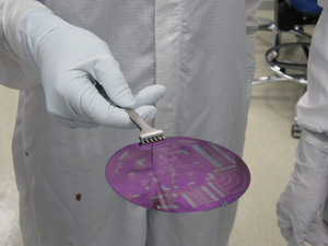
Although similar nano facilities are well-established at Cornell University, Stanford University and UC Berkeley, Nano3 is beginning to distinguish itself through its focus on nanoimprint lithography, a means for rapidly replicating tiny nanodimensional devices for electrical, optical, and biological applications.
The nanoimprint process is relatively simple in concept — it's essentially a mold-patterning process, which works much like a waffle iron.
|
"First you make a mold that has nanodimensional features etched into it," explains Fruhberger. "Then you take a wafer and coat it with soft polymer, push the mold into this polymer and allow the polymer to flow into the etched features. By using heat or ultraviolet light to cure and harden the polymer, it is possible to remove the mold and retain the nanoscale mold features on the wafer. This means we can rapidly reproduce devices at truly nanoscale dimensions. The mold can be used over and over again, with the imprinting process taking less than a minute."
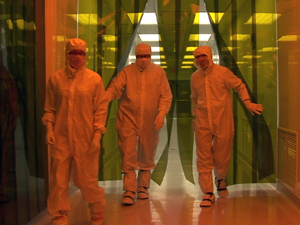
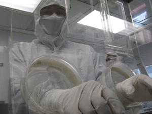
Anyone entering the Clean Rooms at Nano3 can witness the lab's philosophy of cross-collaboration in action: grad students in bioengineering work alongside corporate employees from private companies, sometimes accruing hundreds of hours per week in the lab. But then again, entering the clean rooms is no simple matter - everyone who sets foot in the facility must first go through a stringent preparation in the "pregowning" area, which requires donning shoe-covers, a hairnet, a face mask, and gloves, which is followed by a further set of precautions in the "gowning" area, so that in the end, only the skin around the eyes is exposed to the air.
The gowning procedure can take 30 minutes for the novice, but just a couple of minutes for a veteran clean room user, Fruhberger says. Even after the researchers are decked out in their "bunny suits," a complex regulatory system within the 7,000-square-foot building controls air temperature, humidity, particle quantity, lighting and water flow.
"Ninety percent of the particles generated in clean room space are generated from people, from skin, hair and breath," says Fruhberger. "If you're trying to make a device with nano- or micron-sized features and a piece of dust — typically in the order of a few microns — settles onto it, it can destroy your device. So even though people compliment us on being a very clean lab, it's an ongoing battle. We want to make sure the users are maintaining a safe, clean environment so that everyone's processing can proceed, but we don't want to be overly restrictive or overbearing so people can't get their work done. Personally I think that's one of the biggest challenges — to walk that line properly."
"While we observe certain rules on permitting materials inside the facility, we are purposefully not very restrictive. We may not get the ultimate yield that you'd see in a more restrictive lab," he continues, "but the benefit is that we enable users all the way from biology to engineering and physics and chemistry to process devices. We are ultimately a research and not a small-scale manufacturing facility. Our researches demonstrate proof-of-concept for engineering applications, or build platforms to carry out research on fundamental phenomena in the physical sciences. Having all these various groups working together in a single space creates a level of communication and exchange that is hard to establish at a typical lab."
Researchers affiliated with the lab include Joseph Wang, who joined the faculty of NanoEngineering this summer. Wang, who is consistently one of the world's most cited engineers and chemists, has moved his laboratory for Nanobioelectronics into the second floor of Calit2's Atkinson Hall on the La Jolla campus, and has also installed equipment in the Nano3 facility.
|
Working in the field of nanophotonics are Professors Shayan Mookherjea, Shaya Fainman (both from the ECE department) and Prab Bandaru of the MAE department.
"Nanophotonics is a hot area because it theoretically will enable communications on a computer chip by way of photons rather than electrons," says Clean Room Manager Bernd Fruhberger. "It can revolutionize computing because photons are much faster and do not generate as much heat."
Also from the ECE department are Professors Edward Yu, Paul Yu and Deli Wang, who are working on a joint project in renewable energy to develop high-efficiency solar cells by incorporating semiconductor nanostructures. Also from ECE, Professor Gabriel Rebeiz develops radio-frequency MEMS (micro-electro-mechanical systems) for telecommunications and wireless devices.
MAE Professor Sungho Jin uses the lab for his research in the field of nanomagnetics and nanomaterials fabrication.
"The other area I think could tremendously impact our lives is the utilization of nanotechnology for biomedical applications," adds Nano3 manager Fruhberger. "We have people working on developing nanoparticles for drug delivery, as well as developing devices that allow doctors to target cancers locally rather than throughout the whole body." One group of researchers making strides in the biomedical field includes Professors Andrew Kummel and William Trogler of UCSD's Chemistry and Biochemistry department, as well as NanoEngineering Professor Sadik Esener, who is also the director of the NanoTumor Center at the Moores Cancer Center. The team is using the Nano3 facility to develop automated microscopy system to identify cancer cells in excised breast tumors during cancer surgery to reduce need for multiple breast surgeries.
UCSD Physics Professor Leonid Butov also uses the lab space to develop excitonic signal processing in semiconductor nanostructures to interface optical signal with electronic signal processing. Additionally, Physics Professor Ivan Schuller — one of the lab's founding faculty leaders — says his group is working on research in nanoscience for fundamental devices, superconductivity (specifically, a process known as "artificial pinning"), and sensors for explosives.
Concludes Lo: "It's the people who make a difference. Although we are comparatively small, we are fast growing. We have built up a world-class team of six staff - three of them with Ph.D.'s in chemistry, physics and engineering - and four students devoted to helping users in their research, pushing the frontiers of nanotechnology and sharing their knowhow and experience with users. Our staff work extra hard to not only keep the facility running and well-maintained, but also to work with the users on their toughest processing challenges. We have developed much closer relations with our users than other facilities do. I can hardly think of any university facilities with people of such quality, devotion and enthusiasm."
Media Contacts
Tiffany Fox, (858) 246-0353, tfox@ucsd.edu
Related Links
Nano3
XCom Wireless