UC San Diego Engineers Demonstrate Smallest Laser to Operate at Room Temperature
San Diego, May 3, 2010 -- Imagine packing 4 billion nanolasers on a three-inch semiconductor wafer. That is now nearer to reality, thanks to researchers at the University of California, San Diego’s Jacobs School of Engineering, who have demonstrated a micron-sized laser – less than one-thousandth of a millimeter on each side – that can operate at room temperature.
|
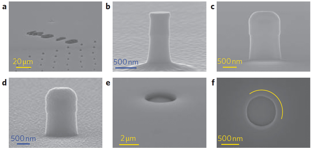
“Shrinking the size of lasers to below their wavelength of emission has been challenging historically,” said Yeshaiahu (Shaya) Fainman, principal investigator on the project and a Cymer professor in UC San Diego’s Electrical and Computer Engineering (ECE) department. “What we have developed is a laser measuring one micron or less in all three dimensions – height, width and depth – that emits a beam with a wavelength of approximately 1.4 microns. These devices are truly ‘subwavelength,’ because they are smaller than the wavelength of light they emit into air.”
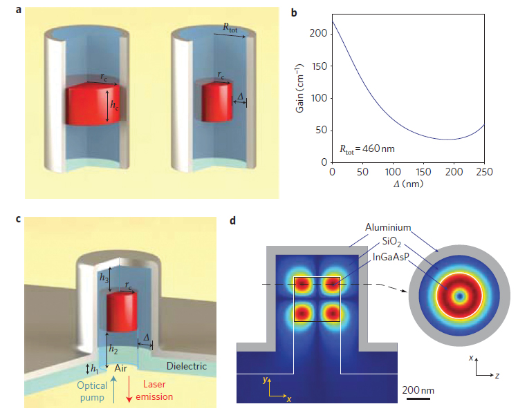
In theory these nanolasers could be packed densely on a wafer because the metallic aluminum layer helps to avoid coupling between neighboring nanolasers and also helps to conduct and dissipate the heat generated in the lasing process. “Using the aluminum shield gives the device superior heatsinking properties, which is important for device operation,” added Fainman. “Using the metal shield confines the optical mode, so that two or more lasers can be placed very close to each other without interfering with each other's operation.”
|
To achieve a subwavelength laser, Nezhad and his colleagues in Fainman’s Ultrafast and Nanoscale Optics Group worked through a series of approaches to create an efficient subwavelength cavity. The conventional approach used in the past for this purpose had been to use a fully dielectric cavity, but it quickly became evident that in the subwavelength size regime this type of cavity would not lead to a working solution. The UCSD team decided to incorporate a metal/dielectric composite layer in the nanolaser design to create an efficient resonant cavity and also to electromagnetically isolate the nanolaser from surrounding devices. The immediate candidates for the metal to be used – aluminum, gold and silver – all have good optical properties because they are very reflective (i.e., they absorb less light). In the tests described in the Nature Photonics article, aluminum was used, but Nezhad says that in theory, silver should be the most efficient shield.
|
The researchers point out that it is of paramount importance to control the thickness of the glass layer. “If you don’t put this glass layer around it, the metal would be too close to the optical field, and there would be too much interaction between the metal and the field and the cavity losses would be too high,” explained Nezhad. “On the other hand, a glass layer that is too thick would result in a device that is either too large or has too little active semiconductor material -- reducing its efficacy. Through careful design, fabrication and testing, we found an optimal balance that created a room temperature laser that emits an infrared beam with a wavelength that is larger than the overall device dimensions.”
Funding for the research came from the Defense Advanced Research Projects Agency (DARPA), with additional support from the National Science Foundation (NSF) and the Center for Integrated Access Networks (CIAN), an NSF-funded Engineering Research Center. Fainman is the Deputy Director of the nine-university collaboration.
|
|
“With an optical pump, an external laser comes in at one wavelength and you excite the gain medium and then collect the light at the lasing wavelength. This requires a fairly large and complicated optical setup,” explained Nezhad. “But if we can achieve these goals with an electrical pump, instead of relying on an external laser, you would only need a tiny power source to fuel the laser.”
Looking ahead, principal investigator Shaya Fainman says the program at UC San Diego aims to accomplish DARPA’s roadmap on time or ahead of schedule. “Making electrically pumped arrays of these lasers is one approach we are already working on, and we will also look at replacing aluminum with silver because of its unique optical properties,” said the Calit2-affiliated scientist. “Another challenge will be to show that the properties of this micron-sized laser will hold up as we pack more and more lasers on a wafer.”
Meanwhile, the teams at other universities are working on their own solutions to the challenges set forth by DARPA, so the researchers at UC San Diego won’t be resting on their laurels.
|
Note to Editors: High-resolution imagery available on request.
---
* "Room-temperature subwavelength metallo-dielectric lasers", Maziar P. Nezhad, Aleksandar Simic, Olesya Bondarenko, Boris Slutsky, Amit Mizrahi, Liang Feng, Vitaliy Lomakin & Yeshaiahu Fainman. Nature Photonics, Advance Online Publication, 18 April, 2010. Published online: 18 April 2010 | doi:10.1038/nphoton.2010.88
Media Contacts
Doug Ramsey, 858-822-5825, dramsey@ucsd.edu or Daniel Kane, 858-534-3262, dbkane@ucsd.edu
Related Links
Nature Photonics Article
UCSD Ultrafast and Nanoscale Optics Group
Nanoscale Architecture for Coherent Hyper-Optic Sources (NACHOS)
DARPA Microsystems Technology Office
Defense Advanced Research Projects Agency (DARPA)


