Researchers Generate Tunable Photon-Pair Spectrum Using a Roomtemperature Quantum Optics Silicon Chip
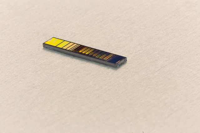
San Diego, December 17, 2014 — A team of researchers from the University of California, San Diego have demonstrated a way to emit and control quantum light generated using a chip made from silicon — one of the most widely used materials in modern electronics.
The UC San Diego researchers recently described their new device’s performance online in the journal Nature Communications, available via Open Access.
The researchers say practical applications of quantum optics will seem more feasible if devices for generating and controlling these photons can be manufactured using conventional materials from the semiconductor industry such as silicon. These devices could have applications in secure communications, precise measurements of motion or shape, and sensing using ultra-low levels of light.

For instance, the researchers suggest that their silicon pair-generation chip could be used as part of a more complicated “quantum transceiver” module, which would eventually integrate a controllable photon source with a sensitive photon detector in a single package.
“Optical transceivers have revolutionized data communications, and tens of millions of these devices are used to send billions of bits of data all over the internet and inside data centers every second,” said Shayan Mookherjea, an associate professor of electrical and computer engineering at the UC San Diego Jacobs School of Engineering. “But these transceivers contain lasers that are made using compound semiconductors, not silicon—which would be more manufacturable and cheaper. The fact that silicon can be used to make a quantum photonic pair source, and that its spectral properties can be fine-tuned easily is exciting from a technological point of view.”
“Silicon is known to be a poor light-emitting material—there is no silicon diode laser, for example, despite many decades of research,” added Mookherjea. “However, if you want to make a chip that emits quantum light such as pairs of single photons which are entangled in some quantum mechanical properties and you want to do it at room temperature so that the chip can be widely used, then it turns out that silicon is actually quite a good material for generating photons.”

How the Nanophotonic Chip Works
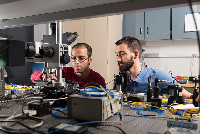
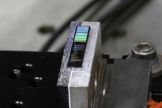
“A beam of light from a laser diode is shone into the chip, and for each pair of photons from the input beam that is absorbed by the material, a pair of photons is produced at two slightly different frequencies—one higher than the input and the other lower than it, such that the total energy is conserved,” explained MarcSavanier, a postdoctoral researcher with the Micro-Nano-Photonics research group at the UC San Diego Jacobs School of Engineering. “Our chip is compact—only millimeters in size—and it works at room temperature, and only requires a simple telecommunications-grade low-power laser diode as the input, and filters to separate the two daughter photons from their parent beam.”
Spontaneous Optical Nonlinear Mixing (SONM), the process of photon creation exploited by the researchers in their device, has been shown in a number of different materials such as glass fibers, crystals, and semiconductors like silicon.
“One thing you have to do, though, is to pattern the silicon into waveguides and micro-resonators which enhance the optical intensity at specific wavelengths,” said Savanier. “These features are less than a micrometer in height and width—far less than the thickness of a human hair, for example. A piece of silicon by itself is not going to have a very high SONM coefficient and it won’t generate a measurable number of entangled photon pairs.”
Varying the Spectrum of the Photon Pair
When a silicon chip is patterned using a process called lithography, features that resemble ridges and valleys are permanently etched into the surface of silicon and many of the properties of the device are fixed. The UC San Diego researchers showed that a particular type of patterned structure allows the quantum mechanical properties of the photon pair to be changed over a wide range, by varying a few simple experimental parameters.

“For example, by varying the chip temperature by only a few degrees, we can tune the degree of entanglement by more than a factor of three, as measured by a typical metric called the Schmidt number,” said Ranjeet Kumar, an electrical engineering graduate student at UC San Diego and lead author of the paper. “A low Schmidt number represents a device generating photon pairs that has been tuned for a particular quantum optic property called heralding, whereas a high Schmidt number shows that the device generates photons which can be used to encode more than a single quantum bit of information per photon.”
“Our device can be tuned over a wide range of Schmidt numbers, whereas other photon pair sources generally cannot, or require complicated additional apparatus to do so—typically thousands of times larger in size than our chip,” Kumar said.
In their work, the researchers show how the degree of entanglement is related to a measurement called the Joint Spectral Intensity (JSI), and describe a technique for measuring the JSI experimentally using single photon detectors.
“Previously, controlling the JSI of a photon pair source required a large assembly of optical components on an optical table, and painstaking alignment of spatial light modulators, cylindrical lenses and mirrors” said Savanier. “This made the photonpair source apparatus bulky, vibration-sensitive, expensive, and not portable. The unique structure of our chip makes this process much simpler, more compact and lightweight.”
The researchers showed that the JSI of the chip can be varied by tuning the temperature of the chip by a few degrees, using compact thermo-electric controllers like those typically used with practical opto-electronic microchips. Alternatively, a typical distributed feedback laser diode used as a pump can tune its wavelength over a few nanometers, which can also alter the JSI.
Jun Rong Ong, also of UC San Diego, joined Kumar, Mookherjea and Savanier as a coauthor on the paper. The research was funded by the U.S National Science Foundation and the U.S. Defense Advanced Research Projects Agency.
Media Contacts
Ioana Patringenaru, Jacobs School of Engineering, 858-822-0899, ipatrin@ucsd.edu
Related Links
Nature Communications article via Open Access
Micro-Nano-Photonics Research Group
Jacobs School of Engineering
Electrical and Computer Engineering Department

