Laser Cavities Take on New Shapes and Functionalities
Researchers have demonstrated the first laser cavity that can confine and propagate light in any shape imaginable, even pathways with sharp bends and angles. The new cavity, called a topological cavity, could enable laser components to be packed more densely on a chip, leading to higher speed optical communication technologies that can be fabricated in an efficient and scalable manner using photonic integration techniques.

WATCH VIDEO
This paper was published online by the journal Science on Thursday, October 12, 2017.
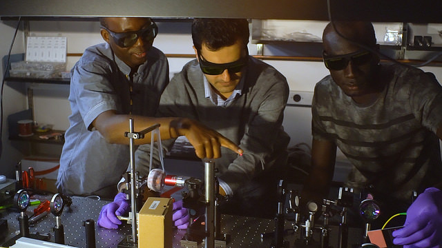
“Our goal is to overcome the fundamental limitations of optical devices and uncover new physical principles that can enable what was previously thought impossible,” said Boubacar Kanté, a professor of electrical and computer engineering at UC San Diego and the study’s senior author.
Kanté is also an academic participant in the Qualcomm Institute (QI), and the groundbreaking work was performed in part at the QI-based San Diego Nanotechnology Infrastructure (SDNI) at UC San Diego.
In most conventional lasers, the laser cavity needs to have a regular curved shape, typically a ring, for light waves to propagate and stay in the cavity. If the cavity has a sharp turn, some of that light gets scattered and lost. This is why, for example, optical fibers can’t have any kinks or bends.
“When you change the shape of the cavity, you change the way light is confined in that cavity,” said Babak Bahari, an electrical engineering Ph.D. student at UC San Diego and the first author of the paper.
Not being able to change the cavity shape also limits how many components can be integrated into a photonic chip. “If we can deform the shape of the cavity, we can easily fit it in any area on a chip without disrupting or moving other components. This would give us more freedom in designing chip components and making denser, more powerful devices,” Kanté said.

Now, Kanté, Bahari and colleagues have introduced a way to make laser cavities of arbitrary shapes without changing their properties.
They created a structure consisting of two photonic crystals, one surrounding the perimeter of the other. The crystal on the inside is grown from the same materials as the crystal surrounding it, but they are what’s known as topologically different—they can be described as having different numbers of holes, like a bagel (one hole) versus a pretzel (three holes). The crystals also exhibit a property in which they can both conduct the same wavelength of light on the outside while acting as insulators on the inside. By putting these crystals together, researchers created a cavity in which light waves can propagate at the interface between the crystals.
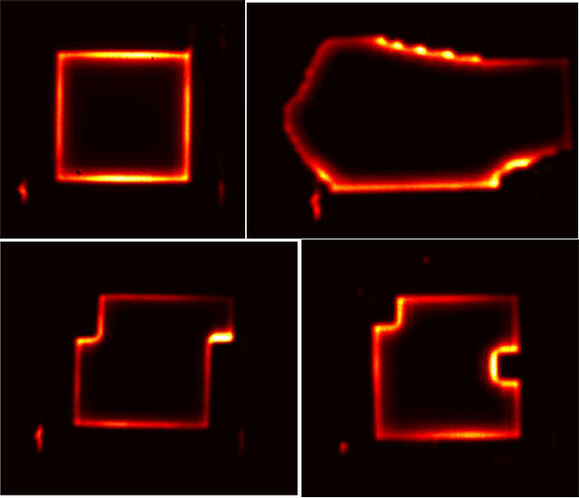
The researchers call this a topological cavity. It is not a space, but the border where two topologically different materials meet, Kanté pointed out. This cavity can be any shape—triangle, square, a loop with jagged edges—and light can circulate within that shape without getting scattered.
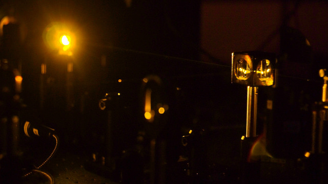
To demonstrate the lasing capability of their device, researchers first coupled a waveguide to the cavity. Then they energized the crystals with light from a high power laser and applied a magnetic field. Using an infrared camera, they observed their device emitting a lower frequency laser beam at 1.55 micrometers, a common wavelength for telecommunications.

Another noteworthy feature is that this device has a non-reciprocal lasing mode, meaning the laser beam can only travel one way. This isn’t the case with most existing lasers, which need a device called an isolator to be placed in front of the source and prevent the laser beam from coming back in and potentially destroying the cavity. Isolators are usually large devices and the new work may thus eliminate the need for them in the future, Kanté said.
“This new feature enables us to make a laser which is self-protected,” Bahari said.
Moving forward, the team hopes to create an electrically powered device, which would make it more practical. Kanté is also planning to further explore the fundamental physics of topological cavities. He is particularly interested in investigating how densely such cavities can be packed on a chip. These studies could be important for quantum information processing and could overcome fundamental efficiency limits of current systems, he said.
###
The team has filed a patent on this technology. Contact Victoria Cajipe in the campus Innovation and Commercialization Office at vcajipe@ucsd.edu or (858) 822-2304 for licensing information.
Paper title: “Non-reciprocal lasing in topological cavities of arbitrary geometries.” Authors of the study are Babak Bahari, Abdoulaye Ndao, Felipe Vallini, Abdelkrim El Amili, Yeshaiahu Fainman and Boubacar Kanté, all at UC San Diego.
This research was partially supported by the Office of Naval Research Young Investigator Award (N00014-17-1-2671), the National Science Foundation Career Award (ECCS-1554021), the U.S. Department of Energy (EE0007341), the National Science Foundation (ECCS-1405234, ECCS-1507146, CCF-1640227), the Office of Naval Research Multi-University Research Initiative (N00014-13-1-0678), the Army Research Office (W911NF-16-1-0245), the Semiconductor Research Corporation, and startup funds from UC San Diego. This work was performed in part at the San Diego Nanotechnology Infrastructure (SDNI) at UC San Diego, a member of the National Nanotechnology Coordinate Infrastructure, which is supported by the National Science Foundation (ECCS-1542148).
Media Contacts
Liezel Labios, Jacobs School of Engineering, 858-246-1124, llabios@ucsd.edu
Related Links

