UCI Receives NSF Grant to Purchase Nanoimprinter
By Anna Lynn Spitzer
08.18.05 – The science of investigating materials on a very small scale took a giant step forward recently. The National Science Foundation awarded UCI nanotechnology researchers $380,000 to purchase a nanoimprinter, an instrument that will help them fabricate a variety of nanoscale-sized new devices. (Nanotechnology is the science of working on a scale smaller than 100 nanometers, or 1/10 of one micron. A micron is one-millionth of a meter.)
|
In the near future, nanopatterned devices will be used in sensors, medical devices, electronics, cars and pharmaceuticals, to name a few. In fact, emerging nanotechnology applications are expected to affect almost every type of manufactured good over the next 10 years.
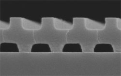
The new nanoimprinter will emboss or transfer polymer patterns onto silicon wafers in a matter of minutes, creating three-dimensional raised surfaces.
These three-dimensional shapes can be used in three ways: to create patterns on an underlying substrate, necessary for the manufacturing of nanocircuits; as functional components for electronic devices; and as tools to understand the physical, chemical and mechanical behaviors of the material at the nanoscale level.
While the nanoimprinter will be used primarily with polymers, researchers will be developing new materials for patterning as well. A byproduct of the nanoimprinting process is the manufacture of nanowires – tiny channels which are 100-200 times thinner than a human hair. Nanowires are expected to become the base of next-generation computing products.
|
Other nanopatterning techniques are currently in use – including photon (light)-based patterning and conventional nanoimprinting – but they are more expensive, slower and less flexible than the nanoimprinting techniques that will be developed at Calit2 using the new equipment.
The nanoimprinter, which is expected to arrive at the Calit2 Building early next year, will have alignment capabilities and features that will increase the yield of each emboss. UCI researchers will be using a wider variety of polymeric materials in creating the nanostructures and they are confident that these new materials, coupled with the new processes that they’ll be developing, will ultimately lead to innovative new devices.
The ability to pattern these features on a nanoscale will benefit many fields, including semiconductor device manufacturing, biotechnology and photonics. Polymer nanoimprinting could help the electronics industry attain resolution requirements necessary for producing next-generation chips; the tiny channels could also be used for transporting fluids or providing treatment for neurological diseases. Studying the role of nanostructure in the adhesion and development of cells also will help researchers better understand diseases like cancer and coronary obstructions.
“Developing an understanding of polymer surfaces and ultrathin polymer films is of fundamental importance,” said Albert Yee, Calit2 Irvine division director, materials scientist and a principal investigator on the new grant. “By studying increasingly smaller structures down to around 40 nanometers, we can deduce the properties of the surface with the help of numerical modeling.”
Calit2’s new equipment will be housed in the building’s clean room, where it will be used by a dozen UCI researchers, and approximately 25 graduate and undergraduate students. Industry partners will also have access to the equipment.


